An Innovative Multilayer PCBA Manufacturer

Custom PCBA Manufacturing Service!

Banner

Cold Solder Joints: Causes, Detection and Prevention Guide

Table of Contents

In industries such as aerospace, medical devices, or heavy industrial control, one hidden cold joint can trigger an accident or an expensive recall. Cold solder joints are one of the most common and critical issues affecting electronic reliability, and such faulty connections can cause intermittent functionality, total shutdown, or gradual component failure in electronic devices. It is essential for every action, whether manufacturing, quality assurance, or repair, to understand cold solder joints to maintain the integrity of the product.
This guide provides explaination on cold solder joints, their identification, root causes, and practical solutions. It also contrasts cold solder joints with other defects like incomplete solder, empty solder, and solder bridges. Let’s follow ELE PCB to get a deep understanding of cold solder junctions!

What is a Cold Solder Joint?

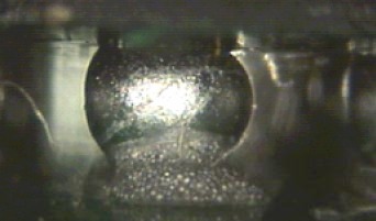
A cold solder joint happens when there is improper bonding between a solder and a solder-surface interface because of either incomplete melting or lack of fusion of the solder. This occurs as a result of surface oxidation, movement during cooling, or low heat. Joints obtained through this process are usually weak and will have a grainy appearance. They will also be susceptible to failure when exposed to stress or temperature fluctuations.
cold-solder-defect
Cold Solder Joint vs Good Solder Joint​

Impact of Cold Solder Joints

The cold solder defect can seriously affect the quality of circuit board soldering and circuit performance.
  • Weak solder joints: Cold solder leads to the joints not being fully melted, resulting in reduced joint strength and an increased risk of falling off or fracturing.
  • Increased resistance: Cold solder joints commonly obtain more pores and impurities, resulting in increased resistance and affecting the circuit’s normal operation.
  • Impeded signal transmission: Cold soldering may lead to signal transmission lines breaking or short-circuiting, affecting the stability of signal transmission.

Types of Cold Solder Joints

Type
Apperance
Hidden Flaw
Failure Trigger
Fractured Joint
have some kind of cracks
Subsurface cracks (X-ray only)
 
Components shift or settle as they cool
Dry Joint
irregular but dull appearance
Organic contamination (FTIR-traceable)
Bad wetting resulting from oxidation or insufficient heat
Grainy or Frosty Joint
rough, crystal-like surface
Tin whiskers (SEM-visible)
A lack of full melting temperature or disturbance during solidification
cold-solder-joint-appearance

How to Identify a Cold Solder Joint

The methods of identifying cold solder joints are as follows:

Visual Inspection

Looking at the joint steadily and slowly with the unaided eye is still one of the fastest ways to get started. Cold joints often appear dull, lumpy, or wavy, and may show spider-web cracks around the edge. In contrast, a good joint shines, looks smooth, and has a gentle, even curve.

Microscopic Examination

On crowded boards or pins packed tight, a low-power loupe or clip-on microscope reveals problems the eye simply misses. Defective solder may patchily wet, tiny trapped bubbles, or a gray-sandy haze across the surface. Each mark shows the molten metal never flowed the way it needed to bond securely.

Electrical Checking

Even a simple multimeter or a basic continuity tester can check sudden jumps in resistance, drop-outs in signal, or outright failure through uncommon wiggle. That uneven response shows the joint never closed completely, so the circuit is fragile and unreliable.

X-ray Inspection

When solder joints are hidden under components such as Ball Grid Arrays (BGAs), X-ray imaging can spot cracks, weak or poorly wetted areas, or connections that do not touch electrically.
Regular scans with this method, especially after hand repairs or wave and reflow soldering, help confirm quality and support the assembly’s long-term reliability.
good-joint-bad-joint-comparison

Root Causes of Cold Solder Joints

Cold solder joints appear whenever the melting metal fails to grip both the component lead and the PCB pad securely.
cold solder joint 2
cold-solder-joint-1

Insufficient Heat

Cold solder joints appear mostly when the iron tip stays too cool or touches the joint only for a split second. The alloy never climbs the liquidus line, instead puddling sluggishly and freezing before fully wetting the surfaces. The result is a brittle, snow-like line that looks dull and fails under moderate stress.

Oxidized Leads or Pads

Any thin layer of oxide interrupts the intimate contact required for reliable wetting. Old components and boards, especially if stored in open air, tend to develop such films on copper or solder-coating surfaces. Consequently, the solder beads up instead of spreading uniformly, and the final joint shows voids or isolated islands that carry almost no mechanical strength.

Movement During Cooling

Any form of shaking or movement can disturb the solidification phase of solder crystallization. This will often result in structural fractures or poor electrical connectivity, which will weaken the solder joint both mechanically and electrically.

Dirty Soldering Materials

Oil, dust, and residues from hand grease, as well as flux, will obstruct the flow of solder and bonding of traces, necessitating high levels of cleanliness. High levels of cleanliness are needed to prevent contamination.

How to Prevent Cold Solder Joints?

Compared to fixing cold solder joints, it’s much easier to avoid it during soldering. Cold solder joints can be all but eliminated when practitioners control heat, cleanliness, and technique at every stage.

Step-by-Step Cold Soldering Best Practice

These are the few steps that need to be taken:
  • First, always work with a calibrated soldering iron so the tip temperature stays steady.
  • Next, thoroughly scrub component leads and PCB pads with isopropyl alcohol or a fine abrasive, removing oxidation and grease that inhibit solder flow.
  • Then apply fresh, low-activity flux in a measured amount-it should bead around the joint without pooling excessively.
  • During soldering, hold components still with tweezers or a fixture, allowing molten metal to bond evenly and preventing movement before solidification.
  • After assembly, run automated optical inspection, spot-heating scans, and other quality checks, catching tiny defects before boards leave the line.
Following this sequence of controls significantly strengthens each joint and cuts the costs tied to field failures and expensive rework.

Special Considerations for BGA/CSP Components

BGA and CSP have a high rate of cold soldering during hot air reflow soldering because the hot air used for heat transfer is difficult to penetrate the small gaps, resulting in low heat transfer efficiency.
In such situations, solutions include:
  • Using a trapezoidal temperature profile to reduce the peak temperature of the reflow in moderation by extending the peak temperature time.

This improves the dissipation of heat capacity components and large heat capacity components, avoiding overheating of smaller components.

  • Improve the supply of heat for reflow soldering.

Reflow soldering involves welding thousands of components onto a PCB substrate. If the PCB is not the same size, has different heat capacities or areas, it will cause uneven temperatures. Infrared heating can be used to uniformly heat the surface of the same object, producing small thermal stress in the welded parts, high thermal efficiency and energy savings.

how-to-fix cold-solder-joints

Comparison: Cold Joints vs. Other Solder Defects

The following table lists the various solder joint defects that can occur during the soldering process, along with their causes and effects:
Defect
Appearance
Electrical Effect
Cause
Cold Solder Joint
Dull, cracked, grainy
Intermittent / Open
Movement or Inadequate heat
Incomplete Solder
Partial coverage
Poor conductivity
The solder application is insufficient
Empty Solder
No solder present
Open circuit
Solder Paste omissions or issues during reflow
Solder Bridge
Unwanted solder bridge
Short circuit
Using too much solder or the spacing between components is poorly executed
incomplete solder vs empty solder vs solder bridge

Cold Solder vs Pseudo Soldering

  • Cold solder joints result from insufficient heat, which causes the solder to fail to fully melt and wet the surface.
  • Pseudo soldering, on the other hand, are often caused by the oxidation of pads or pins, or by ineffective flux. In these cases, the solder melts but fails to bond effectively with the surface.
Visually, cold solder joints appear rough and dull, with visible unmelted solder particles; pseudo soldering, however, look relatively normal.
However, there is a gap between the joint and the contact surface and the bond is not tight, making them prone to intermittent connectivity issues later on.

Conclusion

solder-defect-comparison
Cold solder joints remain a persistent challenge in electronics manufacturing and repair, compromising product reliability through intermittent connections and premature failures. Implementing rigorous process controls—including precise temperature management, oxidation prevention, and movement mitigation during cooling—significantly reduces occurrence rates. For complex assemblies like BGAs and CSPs, specialized thermal profiling and inspection protocols are essential to ensure robust solder connections.
As specialists in PCB quality assurance, ELEPCB provides:
  • Advanced Inspection: Detecting subsurface defects in PCBs to keep high-quality
  • Soldering Process Audits: Identifying and resolving root causes of cold joints
  • IPC-Certified Services: Obtaining ISO9000、ISO9001:2005、ISO14001、UL、TS16949 certificates
Contact our expert team to discuss your specific reliability challenges.

FAQs

A1:Typical indicators are flickering displays, sudden resets, audio dropouts, or sporadic loss of power. Merely tapping the device often restores operation for a moment, showing the joint is not reliably stable.

A2: It can show up over time, especially under frequent heating, cooling, vibration, or gradual oxidation that weakens the bond. Devices kept in harsh, dusty, or humid places are particularly at risk.

A3: First, desolder the bad joint with a pump or wick, then clean the pad and lead, add fresh flux, and resolder while carefully controlling heat, so the new bond solidifies properly.

A4: A digital multimeter, a decent hand lens or small microscope, and the usual soldering kit will cover most cases. For dense or critical boards, X-ray or signal-tracing gear becomes helpful, but rarely essential.

CONTACT US


We provide technical expertise form prototype through production, increasing speed to market by 20%.

                   Contact us below to start discussing your project with our Technical Experts today.

                   Whether you already have Gerber Files, submit a Quick Quote for free estimate.

Youdong Liu
I’m Youdong, a passionate Embedded Systems Designer specializing in custom PCB design and firmware engineering. With a strong background in electronics and IoT product development, I bring innovative solutions to complex challenges. My expertise spans from designing efficient, high-quality PCB layouts to developing robust, optimized firmware. I joined ELEPCB as a full-time technical writer in 2025.
About Benjamin

Benjamin is the general manager of ELE PCB, a leading PCB design and manufacturing company based in China. He has over 10 years of experience in the PCB industry, and has been involved in various projects.

Get a Quote
Recent Posts