

Table of Contents
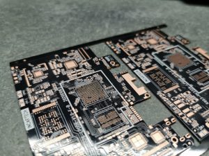
The electronics industry has been transformed due to Printed Circuit Board Computer-Aided Design (PCB CAD) by giving the capability to design highly complex and efficient electronic circuits to engineers and designers. PCBs gives a platform to connect electronic components by using conductive pathways hence act as a backbone of most electronic product.
If you are interested in PCB CAD, follow ELEPCB with the basics of PCB CAD, its significance in electronics design, the tools available, and the steps involved in creating a PCB layout.
What is PCB CAD?
PCB CAD utilizes computer software for the design of printed circuit boards. This software makes it easy to create schematic diagrams, define component placement, and design trace layouts for the engineers. In comparison to traditional PCBs, PCB CAD software erases much of the tedious work that goes into manual PCB creation, providing an automated, precise, and simulation-capable means to design before fabrication.
What's the Difference Between PCB CAD & PCB Schematic?
PCB CAD and PCB Schematic are two different concepts in electronic design.PCB CAD focuses more on physical design and manufacturing, while PCB Schematic focuses more on the logical design and analysis of the circuit.
| Features | PCB CAD | PCB Schematic |
| Definition | Used for the actual PCB layout and design. | A graphical representation of circuit design, showing the electrical connection relationships between components. |
| Function | Mainly used for physical layout, routing, design rule checking, etc. | Mainly used for circuit design, analysis, and simulation. |
| Content | Contains physical design elements such as component packages, routing layers, pads, vias, etc. | Contains logical design elements such as component symbols, connecting lines, net labels, etc. |
| Role | Guides the PCB manufacturing and assembly process. | Helps engineers understand the working principle and performance of the circuit. |
| Design Stage | The later stage, based on the schematic. | The early stage, providing the basis for PCB design. |
| Relationship | Depends on the logical relationships provided by the schematic. | Provides the basis and guidance for PCB design. |
Why is PCB CAD Important?
The importance of PCB CAD lies in the simplification it brings to the process of PCB design.
The major benefits include:
- Accuracy: It guarantees the accurate positioning of components and trace routing.
- Simulation: It provides an opportunity for testing circuits virtually, thereby decreasing the chances of error.
- Efficiency: Reusable templates and libraries facilitate faster design time.
- Complexity Handling: It makes it possible to design multilayer PCBs for complex electronics.
- Cost-Effectiveness: Prototyping is reduced as issues are detected during the design stage.
Features of Modern PCB CAD Software
Modern PCB CAD tools have a number of features that help designers:
- Schematic Capture: Makes it easier to create circuit diagrams.
- Layout Design: Provides tools for defining board shape, trace width, and component spacing.
- 3D Visualization: It aids designers visualize the final product by giving a 3D view.
- Design Rule Checking (DRC): It assures that the design complies with manufacturing requirements.
- Integrated Libraries: Has a library of components with specifications.
- Simulation and Analysis: Provides signal integrity analysis, thermal simulation, and power distribution.
Best PCB CAD Software
Some of the Most Popular PCB CAD Tools are:
- EAGLE: For professionals and hobbyists; it offers schematic capture and PCB layout tools.
- OrCAD: Suitable for high-performance design with demanding specifications.
Want to learn more about PCB design software?
Check out this blog written by ELEPCB!
- KiCad
- Altium Designer
- DipTrace
- LibrePCB
- EasyEDA
Steps for PCB Design with CAD Software
1. Define Requirements
- Firstly, measure the board size, quantity of layers, and component ratings.
2. Schematic Design
- Prepare circuit schematics through the schematic editor of the software.
3. Component Placement
- Set components in the PCB design, considering the space and functions.
4. Trace Routing
- Solder components with copper traces and ensure optimal signal flow.
5. Design Rule Check
- (same as above)
6. 3D Visualization and Review
- Have a look at the 3D board to make sure that everything matches the design.
7. Export Files for Fabrication
- Create Gerber files and other outputs needed in manufacturing.
Check out this blog for the full process of
Gerber files.
2 Special Tips
Tip 1-Component Placement:
- Designers can make use of the user created PCB library.
- User created pcb library may be employed containing customized components that might not originally be part of the ‘default library’ in the CAD package being used.
- It can include components that are especially designed or sourced for a particular project, thus allowing more flexibility in component selection and placement.
Tip 2-3D Review:
- The top view in 3D design of PCB CAD design is quite significant. It allows the designers to get a clear understanding about the layout of components in a printed circuit board from a certain angle.
- This allows, for instance, fast recognition of the position of various parts relative to each other and positioning them in a manner that is functionally and spatially efficient.
- This top view in 3D design of PCB CAD design also helps to double check the routing paths, ensuring that between the components, connections are precisely made without crossovers or short circuits, which may not be so obvious in other views.
Conclusion
PCB CAD software has transformed the electronics design process by making it more effective, precise, and accessible. These tools provide the capabilities needed to bring your ideas to life whether designing a simple single layer board or a complex multilayer PCB. By using the power of PCB CAD, engineers can focus on innovation while reducing costs and time to market.
Contact ELEPCB to find the best solution for your PCB CAD design!
FAQs
A1: The process of drawing a diagram that represents the electrical connections between components is involved in schematic capture and, while PCB layout is concerned with the physical placement of PCB components and trace routing on the board.
A2: Yes, but KiCad and EAGLE are examples of tools that are free or very inexpensive for professional applications, but have fewer features compared to a commercial software.
A3: A PCB can be manufactured with anywhere from a single layer up to over 20 layers depending on how complex a design is. In high computational technology, the PCB can have up to 100 layers or more.
A4: Actually, that is not mandatory as simulation facilitates finding the possible failures in case the PCB under design behaves abnormally even before commencing its fabrications as well.
References
- Official documentation for Altium Designer, EAGLE, and KiCad.


CONTACT US





 English
  Italian
  Hungarian