

Table of Contents
1. Delamination
Delamination is a critical quality issue that can significantly impact the structural integrity and performance of PCB products. It refers to the separation or detachment of different layers within a PCB, resulting in reduced electrical conductivity, compromised signal integrity, and potential failure of the circuit board.
- Dealing with moisture: vacuum conductive bags or aluminum foil bags can be good protection against water vapor intrusion, while the bag is required to put the humidity indicator card. If the humidity card is found to exceed the standard before use, baking before going online can usually solve the problem, baking conditions are usually 120℃, 4H.
- PCB reliability testing: In order to minimize the occurrence of such problems, special attention needs to be paid to the PCB supplier’s management of the corresponding processes and layering reliability tests. Take the thermal stress test in the reliability test as an example. A good factory’s passing standard requires that there be no delamination more than 5 times, and it will be confirmed at the sample stage and each cycle of mass production, while an ordinary factory’s passing standard may only be 2 times. The IR test of simulated placement can also prevent the leakage of defective products, which is a must for excellent PCB factories.
- Optimizing PCB design: Of course PCB design can also bring the hidden danger of delamination. To minimize the risk:
- Use high glass transition temperature (Tg) materials: Employ PCB substrates having a glass transition temperature (Tg) of 145°C or more, especially for lead-free processes. This improves thermal resistance and eliminates layer separation.
- Optimize the copper layout: Avoid large exposed copper areas and highly dense buried via regions, which introduce stress points and promote delamination.
- Design for thermal reliability: Maintain copper distribution in equilibrium and adequate layer piling to reduce thermal expansion variations board-to-board.
2. Poor Solderability
Poor solderability refers to a condition where the solder does not properly adhere to the intended areas on a PCB, resulting in weak or unreliable solder joints. Possible issues are:
ENIG Black Pad
Black Pad is believed to be caused by a phenomenon known as nickel corrosion or nickel phosphorus depletion. It occurs when the nickel layer in the ENIG finish becomes brittle, porous, or non-adherent due to inadequate processing or the presence of impurities. As a result, the gold layer on top of the nickel may appear black or dark, indicating poor solderability and reduced reliability.
Preventing and mitigating Black Pad requires careful attention to the entire ENIG surface finishing process.
Solutions:
Solder Mask Scum
Solder mask scum, also known as solder mask residue or solder mask contamination, refers to the presence of unwanted material or residue on the solder mask surface of a printed circuit board (PCB). It appears as a thin layer or spots of foreign substances, such as dust, oils, or other contaminants, which can negatively impact the functionality, reliability, and aesthetics of the PCB.
Solutions:
3. PCB Warping
PCB board warping refers to the condition where a printed circuit board (PCB) exhibits a non-flat or deformed shape. Instead of being flat and rigid, the PCB may have a noticeable bend, twist, or curvature. This warping can occur during the manufacturing process or as a result of environmental factors or stress applied to the PCB.
Causes of PCB board warping:
(1) Inconsistencies in the manufacturing process, such as improper material selection, inadequate temperature control during lamination or soldering, and uneven distribution of copper layers, can lead to differential expansion or contraction and result in PCB warping.

The consequences of PCB board warping can include:
- Component Misalignment: Warping can cause component misalignment, making mounting and soldering difficult, resulting in weak solder connections and potential component breakage.
- Electrical Shorts or Opens: Warping can produce inadvertent contact or separation of traces, resulting in shorts or opens that can degrade circuit performance.
- Mechanical Fit Issues: Warped PCBs may not fit properly in their enclosures, compromising the final product’s performance and dependability.
- Use High-Quality Materials: Choose high thermal stability and low water absorption substrates.
- Control Lamination and Soldering: Use uniform temperature and pressure in lamination, reflow, or wave soldering.
- Optimize Copper Distribution: Avoid uneven copper layers or excessive copper planes that can cause stress.
- Proper Storage and Handling: Store PCBs in humidity-controlled storage and assemble boards gently.
4. Exposed Copper
Exposed copper that is unintended or outside of the designated areas can result in several problems. It can lead to unintended electrical connections, short circuits, or inadequate isolation between different circuit elements. Exposed copper areas that lack proper solder mask coverage are susceptible to oxidation, which can affect the solderability and long-term reliability of the PCB.
- Offer correct solder mask alignment and full coverage to avoid unintentional exposure of copper.
- Employ finishes such as ENIG, OSP, or HASL to cover exposed copper areas against oxidation.
- Monitor etching and cleaning operations so that over-etching or inadequate mask coverage is prevented.
5. Poor Impedance
Poor impedance refers to a condition in which the impedance of a transmission line or an electrical circuit deviates from the desired or specified value. Impedance is a measure of opposition to the flow of electrical current in a circuit and is typically characterized by resistance, inductance, and capacitance. This can lead to various issues and consequences, including:

The impedance of PCB is an important indicator related to the radio frequency performance of mobile phone boards. A common problem is that the impedance difference between PCB batches is relatively large. Since impedance test strips are usually made on the edge of the large PCB board and are not shipped with the board, the supplier can be asked to pay the batch of impedance strips and test reports for reference each time it is shipped, and it is also required to provide comparative data of board edge wire diameter and board internal wire diameter.
6. BGA Solder Voids
BGA solder voids refer to the presence of empty spaces or gaps within the solder joints of a ball grid array (BGA) component. A BGA is a type of surface-mount integrated circuit package that uses an array of solder balls on the underside of the package to establish electrical connections with the PCB.


This type of failure may occur due to residual liquid or impurities in the PCB holes that vaporize after high temperature, or poor laser hole pattern on the BGA pad. The voids appear as trapped air or gas pockets within the solder material. These voids can vary in size, shape, and distribution, ranging from small isolated voids to large interconnected voids.
BGA solder voids may cause malfunction of the main chip and may not be discovered during testing, so the hidden risk is high.
- X-ray inspection for voids and quality solder joints. As such, the majority of patch factories now X-RAY inspect after mounting parts.
- Electroplate or partially fill vias to avoid air entrapment when soldering. Most HDI boards today require electroplating to fill holes or semi-fill holes in order to avoid this problem.
- Use high-activity solder paste and consistent, quality solder balls to enhance filling and joint reliability.
7. Solder Mask Blistering
Solder mask blistering or falling off refers to a condition where the protective solder mask layer on a printed circuit board (PCB) exhibits abnormalities such as bubbles, blisters, or peeling, and in severe cases, the solder mask layer detaches from the PCB surface.
- Use solder mask ink compatible with high-temperature flux and restrict curing temperature and time to prevent blistering.
- To prevent introducing batch issues, PCB manufacturers have to develop corresponding reliability test requirements and control them in different stages.
8. Via Fill Material Defects
Via fill material, also known as a via filling compound or via fill resin, is a non-conductive material used to fill vias on a printed circuit board (PCB). Via fill material defects refer to abnormalities or issues associated with the material used to fill vias on a printed circuit board (PCB). Via filling is a process where non-conductive material, such as epoxy or resin-based compounds, is injected or applied to fill the vias, isolating them from other conductive layers.
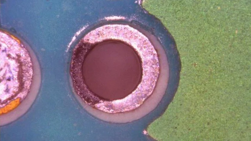
This is mainly caused by the PCB factory’s lack of technical capabilities or simplified processes. They are manifested as incomplete via filling and exposed or false copper exposure in the annular rings. It may cause problems such as insufficient solder volume, short circuit with the patch or assembly device, and residual impurities in the vias. This problem can be discovered during appearance inspection, so it can be controlled during incoming material inspection, requiring the PCB factory to improve it.
Via fill material defects can have various implications on the performance, reliability, and functionality of the PCB. They can affect signal integrity, power delivery, mechanical stability, or resistance to environmental factors such as moisture, temperature, or vibration.
9. Poor Dimensions
PCB dimensional issues refer to problems or deviations in the physical dimensions and measurements of a printed circuit board. These issues involve variations or discrepancies in the size, shape, or positioning of the PCB and its components, which can impact the functionality, assembly, and reliability of the board.
There are many possible reasons for poor dimensions. The PCB production process is prone to expansion and contraction. The supplier has adjusted the drilling program/graphic ratio/forming CNC program, which may cause problems such as easy placement deviation and poor coordination of structural parts. Since such problems are difficult to detect and can only rely on the supplier’s good process control, special attention needs to be paid when selecting suppliers.
(1) Design Verification: Thoroughly reviewing the PCB design and conducting design rule checks (DRC) and design for manufacturing (DFM) analysis to ensure proper dimensions, tolerances, and component footprints.
(2) Manufacturing Process Control: Implementing strict process controls during PCB fabrication, such as accurate temperature and pressure control during lamination, precise etching and drilling processes, and careful handling, can help minimize dimensional variations.
(3) Inspection and Testing: Conducting visual inspections, dimensional measurements, and verification checks throughout the manufacturing process to identify and rectify any dimensional issues before further assembly or testing.
10. Galvanic Corrosion

PCB Quality Issues: Summary Table
| PCB Issue | Main Causes | Solutions |
| Delamination | Improper material, poor lamination, moisture, low Tg material | Use high Tg materials, vacuum packaging, baking before use, supplier testing |
| Poor Solderability | ENIG black pad (nickel corrosion), solder mask scum, contamination | Strict ENIG process control, surface cleaning, use high-quality chemicals |
| PCB Warping | Uneven copper layers, thermal stress, moisture absorption, mishandling | Material selection, lamination control, proper storage, careful assembly |
| Exposed Copper | Incomplete solder mask coverage, poor factory process control | Better solder mask design, strict inspection, supplier quality management |
| Poor Impedance | Design flaws, process inconsistencies, lack of impedance testing | Impedance control in design, supplier test reports, edge/cross-section testing |
| BGA Solder Voids | Residual liquid/gas in vias, poor hole plating, assembly issues | X-Ray inspection, via plating fill, better hole design |
| Solder Mask Blistering | Low-quality ink, improper curing, excessive heat during assembly | Use high-grade ink, process control, supplier reliability testing |
| Via Fill Defects | Incomplete resin fill, false copper exposure, impurities | Incoming inspection, strict supplier QC, improve via filling process |
| Poor Dimensions | Expansion/contraction, CNC/drilling ratio errors, process variation | DFM checks, process control, dimensional inspection |
| Galvanic Corrosion | Gold-copper interaction in OSP process, potential difference | Pre-compensated design, limit rework, supplier process screening |
An Introduction to ELEPCB Factory
ELE PCB factory focuses on high-precision and difficult HDMI and multi-layer PCB board production, with a monthly production capacity of up to 25,000 square meters.
With 7 high-speed SMT lines and 2 THT lines, equipped with advanced equipment such as 3DSPI, X-RAY, and multi-temperature zone reflow soldering, we are able to ensure the production of high-precision products.


The factory production lines have anti-static measures, and more than 95% of our production lines are skilled workers, who have extensive experience in assembling electrical components. The production equipment includes electric pneumatic tools, short circuit equipment, multimeters, ammeters, torque testing equipment, electric bridges, etc., all to ensure the smooth progress of production.
Our production line meets 5S requirements and can complete one-stop services of PCB design, PCB Fabrication, PCB assembly and box build assembly. We can arrange special line production and have a strict quality management system. Each production line has experienced employees and dedicated line follow-up personnel to ensure error-free production.
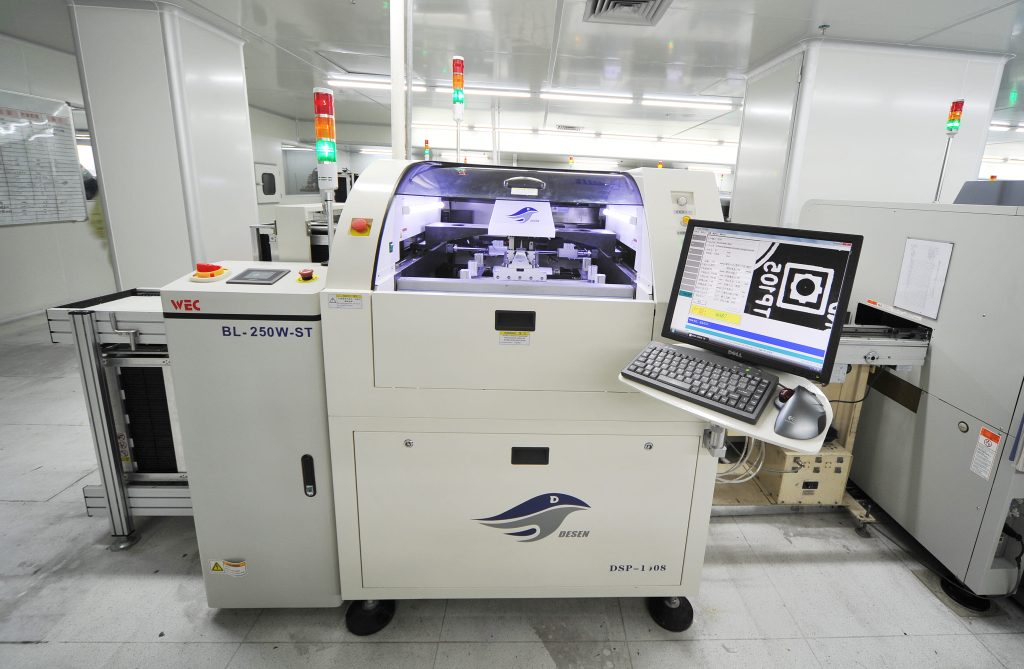
ELE factory will confirm the EQ with the customer before production, and only start production after confirmation. Our corporate culture emphasizes quality first, and we have almost never had major problems with quality.
FAQ


CONTACT US


 English
 Italian
 Hungarian