An Innovative Multilayer PCBA Manufacturer

Custom PCBA Manufacturing Service!

Banner

Bow and Twist of PCBs: Complete Analysis and Solutions

Table of Contents

 It is critical to maintain PCB flatness for component placement, soldering and long-term reliability. Bow and twist are two common types of PCB warpage phenomena that may appear during processing, storage, or assembly. In this article, ELE PCB explains what bow and twist are, how they’re defined in manufacturing standards, and how to get flat and reliable PCBs.

What is Bow and Twist in PCBs?

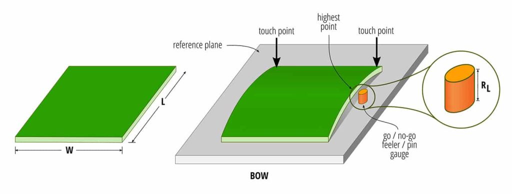
Bow is the term for an even curve from one end of the board to the other. So, it’s the board in a mild arc, forming a shallow “U” shape.
Twist is a twist of the corners of the board so they are no longer in the same plane and the board has a corkscrew shape.
Both defects are categorized as warpage problems concerning PCB flatness and may lead to a wrong component position, an open solder joint or even a short circuit.

Why is Controlling PCB Warpage Important?

Significant bowing or twisting in the shape of printed circuit boards causes a number of problems during manufacture, assembly and performance of the board:
Affect assembly efficiency: Substandard PCB flatness can hinder the positioning of smaller surface mount components and prevent component leads from fitting properly in plated through holes, which will directly increase assembly errors and lower manufacturing yield.
Reducing reliability: Not only warpage causes immediate assembly problems, it also affects the reliability and performance of the PCB over time. Continued stress and misalignment can lead to gradual failure, resulting in degraded performance and early product failure.
Risk of damage during assembly: Incorrect mounting may lead to component damage or misalignment of parts, further affecting the overall quality of the board.
Electrical Exposure Problems: PCB bowing and twisting can also cause electrical contact problems such as broken vias or poor solder joints.
PCB warpage

The Acceptable Limit of PCB Warpage

Since bow and twist are mostly inevitable in PCB manufacturing, controlling them within acceptable limits should be the goal rather than striving to totally eradicate them.The industry follows IPC-A-600 or IPC-6012 to define the acceptable levels of bow and twist tolerance in PCBs.
IPC-A-600: Allows for up to 0.75% SMT board warpage and 1.5% Through-Hole and Mixed MTEG.
IPC-6012: Specifies the requirement of qualification and performance. Establishes limits of flatness for final boards.
The detailed standards and formula to calculate the warpage are below:
 BowTwist
 Limit percentageCalculation formulaLimit percentageCalculation formula
Circuit Board (without SMD parts)1.50%

Longer Side:
RL = L x B / 100

Shorter Side:
RW = W x B / 100

L = Board Length
W = Board Width
B = % Bow Limit

RL & RW = Go/No-Go feeler/pin gauge size for PCB length & width respectively

1.50%

R = 2 (D)(T)/100

D = Diagonal MeasurementT = % Twist LimitR = Go/No-Go feeler/pin gauge size

Circuit Board (with SMD parts)0.75%0.75%
calculate-bow
How to Calculate PCB Bow
how to calculate PCB twist
How to Calculate PCB Twist

What Causes PCB Bow and Twist?

Identifying the root cause of warpage is critical to ensuring the successful production of high-quality PCBs. The common causes of bowing and twisting are as follows:
Material Imbalance (Unequal Copper or Dielectric Layers): An optimal PCB design has IO power distribution over copper and dielectric thickness. If one side of the board is heavily copper-weighted, or has thicker dielectric layers, it introduces uneven mechanical stress during thermal cycling.

Imbalanced Panel LayoutIn case heavy parts or copper traces are not uniformly distributed over the PCB layout, this results in local weight and heat unbalancing. This may distort the board during soldering. Also, non-regular panelization and cutouts can generate stress at a specific point, which may cause twist or bow effect.

Uneven Cooling from the Lamination or Soldering: The PCB stack-up may involve materials with varying coefficients of thermal expansion (CTE). In PCB manufacturing, several layers are combined to form an integral system by pressing together using heat and pressure (laminating). If one side cools more quickly than the other, the difference in temperature creates stresses that can cause the board to warp or twist.
Water Adsorption in Storage: PCBs use materials such as FR4 that can absorb moisture. If the critical temperatures are exceeded, the layers generate steam (by evaporation of the entrained water) and pressure, there’s a popcorn explosion within the layers. If the board is still subjected to high heat (such as reflow), it can cause delamination, warping and even cracking.
Inadequate Handling Pressure: Careless processing such as stacking without support, flexing during inspection, or storing them by standing them on end can cause permanent deformation. Even relatively weak forces sustained over a length of time (such as the weight of stacked units without flat support) can introduce micro-bending, which, in turn, is developed into macro-bow or twist during thermal processing.

How to Get Flat and Reliable PCBs?

The requirements for PCB warpage control have become increasingly stringent with the trend of SMT and chip mounting. How can we keep the flatness of PCBs to ensure its quality?

Ways to Minimize Bow and Twist

ways to minimize PCB bow and twist

Design Process

Maintaining the PCB layout’s symmetry helps in distributing the manufacturing process’s thermal stresses. The methods involve:

  • Balancing the copper pattern and circuit area of each layer of the board.
Make sure the copper (distribution layer) and the dielectric layers are symmetric. Avoid using very high copper layers on one side. Designers must also manage thermal distribution, assembly dispersion, and component layout to reduce warpage. For stress relief, allow routing clearances and processing locator holes.
  • Ensuring boards of layers are products of the same company.
The boards of multiple-layer PCB should have the same specifications to keep the quality. If the thickness of boards is different, they’re easy to get out during the lamination.
The PCB manufacturer must select the most durable prepregs and core, and the buildup must be 100% symmetric, in order to obtain increased stability. ELE PCB provides professional PCB design service and our experienced experts will ensure the layouts’ practicability.
wrong stackup
Manufacturing process
  • Select Proper Materials
Choose laminates with similar CTE (coefficient of thermal expansion) and high Tg to sustain thermal stress.
  • Pre-bake Boards When Needed
For moisture-sensitive boards, pre-baking (chamber) at 120–150°C can dry the board, reducing the risk of deformation in reflow.
  • Heating and Cooling Control
Make sure heating and cooling ramps stay within material limits. Apply steady heat and pressure during the pressing process and cooling must be uniform to avoid tension.
Storage Process
  • Maintain Proper PCB Storage
Store PCBs in suitable temperature conditions. Store them in flat trays (no leaning), keep undercover and enclosed (dry), and do not leave them where they can absorb moisture.

Methods of Fixing Bow and Twist

If the PCBs are warped, it’s better to find the resons and try to aviod these actions in the next time. However, if the value of the board is high, there are several methods below for reference:
Re-bake and Flatten
Put the twisted-up PCB between two flat pieces of metal or in a press and bake at a modest temperature. This may release internal stresses and bring the material back into flatness.
Prototype Flattening by Hand
If it’s less critical (or a prototype), you can use a heat gun and clamps to carefully flatten the board. Not recommended for production systems.
Mechanical Pressing with Heat
Warpage can be corrected at industrial PCB repair facilities using heated pressing systems. This technique needs strict supervision to avoid delamination.
Solder Paste Adjustment
In the case where the warpage is minor, employing the adjustable thickness of the stencil or the volume of the solder paste makes it possible to level the difference in height and complete mounting.

Conclusion

PCB bow and twist can cause serious alignment and operational challenges during the production of PCB. The origins and appropriate corrective measures during design, manufacturing, and storage can be greatly minimized.
Utilizing high-precision processes and reliable substrates, in combination with strict temperature control systems and multi-layer lamination technology, ELE PCB ensures full-process PCB warpage detection for industry-leading flatness. Our ultra-low deformation rate guarantees product reliability and facilitates your design of electronic projects.
 Contact us to get your high-quality PCBs!

FAQs

A1:

The three-point method, shadow moiré method, and laser scanning are commonly used techniques to measure PCB warpage.
A2:
Yes. Twisted boards lead to part placement being out during pick-and-place. SMT machines require a level surface; if it gets warped, parts will be out of place and you’ll end up with poor solder joints. It can be fixed with:
Flat surface and feeler gauges to test for warpage.
The boards can be pre-baked and re-pressed flat.
A3:
Absolutely. FR4 and other laminates can absorb moisture. Moisture turns to steam during reflow, which generates internal pressure and can also deform the parts.
A4:

Yes. Thicker boards (e.g. 2.0 mm vs. 1.6 mm) are stiffer and less prone to warping. But that increases cost, and impedance or weight can be an issue. Only use it if:

Your app requires it (e.g. power boards).
You can’t just rework the appearance of stack-up symmetry.

CONTACT US


We provide technical expertise form prototype through production, increasing speed to market by 20%.

                   Contact us below to start discussing your project with our Technical Experts today.

                   Whether you already have Gerber Files, submit a Quick Quote for free estimate.

Youdong Liu
I’m Youdong, a passionate Embedded Systems Designer specializing in custom PCB design and firmware engineering. With a strong background in electronics and IoT product development, I bring innovative solutions to complex challenges. My expertise spans from designing efficient, high-quality PCB layouts to developing robust, optimized firmware. I joined ELEPCB as a full-time technical writer in 2025.
About Benjamin

Benjamin is the general manager of ELE PCB, a leading PCB design and manufacturing company based in China. He has over 10 years of experience in the PCB industry, and has been involved in various projects.

Get a Quote
Recent Posts