

Table of Contents
ELEPCB’s PCB manufacturing process always attaches great importance to any tests conducted for the quality of PCB.
What is PCB Burn-in Testing?
Definition of PCB Burn-in Testing
Burn-in testing is a process that subjects PCBs to conditions that are more extreme than the normal operating conditions. These conditions can include high temperature, high voltage, high current, high frequency, or high power. The duration of burn-in testing can vary depending on the PCB requirements, but it typically ranges from 40 to 160 hours. The purpose of burn-in testing is to stress the components and connections of PCBs to the point of failure or near-failure, and then inspect and analyze the results.
Definition of PCB Burn-in Testing
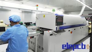
Burn-in testing requires specialized equipment and machines that can generate and control the desired conditions. These equipment and machines are called burn-in testing machines or chambers. They can vary in size, shape, and features, depending on the type and number of PCBs that need to be tested. Some of the common features of burn-in testing chambers are:
| Feature | Description |
| Temperature Control | -40°C to 150°C. Wider ranges accommodate more stress profiles. |
| Voltage Control | 0V to 1000V. Higher voltages induce more electrical stresses. |
| Current Control | 0A to 100A. Higher currents generate enhanced thermal aging effects. |
| Frequency Control | 0Hz to 100MHz. Higher frequencies emulate RF environments. |
| Environmental Conditions | Temperature, humidity, altitude. Replicate climatic conditions PCBs may face. |
| Monitoring Sensors | Temperature, voltage, current, vibration |
| Sensor Inputs | Detect and log parameter changes over time to catch degradation trends. |
| Control Modes | Manual, programmed profiles |
| Profiles | Customizable stress sequences for static or dynamic accelerated aging simulations. |
Notice: This table shows key technical specifications and capabilities commonly found across various burn-in testing equipment to subject PCBs to rigorous controlled stresses.
The Importance of Burn-in Testing
Burn-in testing is an important part of PCB quality control processes. It has several benefits and advantages for ensuring PCB quality, such as:

How to Perform a Burn-in Test?
PCB Burn-in Testing Preparation
Before conducting burn-in testing, it is important to prepare the PCBs properly. Some of the steps and procedures involved in preparing PCBs for burn-in testing are:
- Installing the ICs on the PCBs. The ICs are the main components that are tested during burn-in testing. They are installed on the PCBs using sockets, clips, or soldering.
- Setting the temperature, voltage, current, frequency, and power levels. Remember not to stress the PCBs too high to damage them irreversibly.
- Loading the PCBs into the burn-in testing chamber. The PCBs should be loaded securely and properly into the burn-in testing chamber, connected to the power supply and the signal source, as well as the monitoring and measuring devices. The PCBs should be arranged in a way that allows adequate airflow and heat dissipation.
Starting the Burn-in Testing Process
The burn-in testing chamber is turned on and the conditions are applied to the PCBs. The PCBs are stressed under the controlled conditions and the power supply and the signal source are activated.
- Thermocouples
- Voltmeters
- Ammeters
- Oscilloscopes
- Multimeters
Inspecting and Analyzing the Burn-in Testing Results
Types of PCB Burn-in Testing
Static Burn-in Testing
- Thermal resistance. It can test the ability to withstand high temperatures or temperature cycles without cracking, burning, or deforming. This can ensure that the PCBs can operate properly in environments that have high or varying temperatures, such as automotive, aerospace, or industrial applications.
- Electrical resistance. This can ensure that the PCBs can function correctly in situations that have high or fluctuating voltages, such as power supply, communication, or medical applications.
Dynamic Burn-in Testing
Common Applications of Burn-in Testing
Defense Electronics
Medical Devices
Automotive Systems
Conclusion
FAQ


CONTACT US



 English
  Italian
  Hungarian