

Tartalomjegyzék
Have you considered what each of the thousands of smart devices operating via different communication protocols uses to connect? Have you thought about how industrial hardware, smart house systems, and healthcare devices can communicate with each other even with limited cloud access? This all comes down to the Smart Gateway PCB, which is the brain of IoT networks of today.
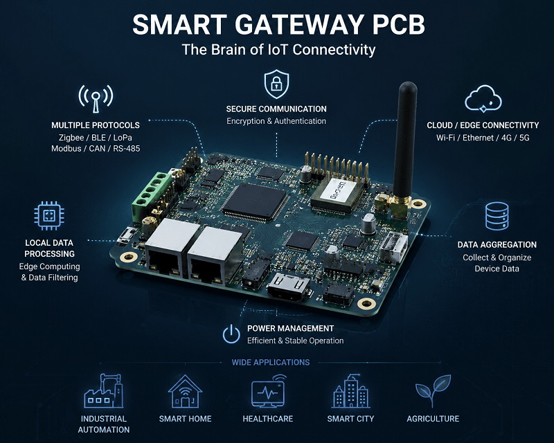
Smart Gateway PCB enables seamless communication at the hardware level by integrating communication, computational, and security functions into one hardware device. Understanding the smart gateway PCB as well as its types, functioning principles, inner components, design issues, challenges, applications, and production processes is fundamental to its functionality.
What is a Smart Gateway PCB?
Smart Gateway PCB is an advanced nyomtatott áramköri lap that acts as an important connectivity device in an Internet of Things (IoT) system. This board connects various devices via multiple wired and wireless technologies and carries out local data processing. It processes and compiles érzékelő data, and sends processed information to the cloud or edge devices in a secure manner. Smart Gateway PCBs have computing, networking, and power management circuits that support effective and intelligent performance in different IoT applications.
Smart Gateway PCB Types (By Construction Type)
Smart Gateway PCBs are designed to fit specific application needs, operating conditions, installation space, and required performance. The construction of the board determines its type, and among the most common types of PCBs used in the manufacturing of Smart Gateway PCBs are rigid, multilayer, flexible, and rigid-flex.
Merev PCB-k
One of the leading types of PCB used in Smart Gateway devices is a merev PCB because of its affordable manufacturing process and high mechanical strength. Rigid PCBs are often employed in industrial communication gateways, smart home hubs, and communication controllers, where there is sufficient space in the device casing and where PCB bending does not occur. Their highly reliable design structure allows proper and steady installation of the circuits controlling the processors, memory, communication components, and power supplies.
Többrétegű PCB-k
Többrétegű PCB-k consist of several layers of copper separated by insulators. Their design allows engineers to incorporate high-speed digital signal transmission, RF communication wires, and power distribution in a compact PCB. Multi-layer boards of Smart Gateway devices usually have 4, 6, or 8 layers to increase signal integrity, lower elektromágneses interferencia (EMI), achieve stable grounding, and ensure the correct operation of complex processors with several wireless connections.
Rugalmas PCB-k
A rugalmas PCB is made of circuit materials that can be bent and used in any irregular casing design, reducing the need for connection parts and making the devices lighter. Such boards can absorb main vibrations and are perfect for small-sized architectures and wearable devices.
Rigid-Flex PCB-k
Rigid-flexible printed circuit boards (PCBs) feature rigid parts used for the installation of the electronic devices, and flexible sections are responsible for the elimination of wiring systems. The considered PCB design increases the reliability of the whole construction and makes assembly easier. Rigid-flex PCBs have become common in advanced automation, aerospace, health care, and compact intelligent devices, which require high durability and flexibility of the design.
How Does the Smart Gateway PCB Work?
The Smart Gateway PCB serves as a device that connects field devices and cloud services through the gathering of data, its processing, and secure forwarding over multiple communication networks. The working process can be divided into the following stages:
Stage 1. Collection of Data
In this stage, the gateway receives data transmitted from sensors, controllers, and IoT devices through communication standards, e.g. Zigbee, Bluetooth Low Energy (BLE), LoRa, Modbus, CAN, or RS-485. Similar devices keep delivering information about the environment, machines, and processes.
Stage 2. Protocol Translation
In the majority of cases, the devices that work in a network use different communication standards, and the gateway is responsible for translating data from one protocol to another. Thus, it provides transmission of information from Zigbee or LoRa protocols into Wi-Fi or Ethernet protocols, for instance.
Step 3: Local Data Processing
Instead of transferring all raw data directly to the cloud, the onboard processor executes edge computing functions such as filtering unnecessary data, evaluating sensor information, identifying unusual events, and carrying out pre-programmed control procedures. Thus, latency and network bandwidth are reduced.
Step 4: Data Aggregation
The information received from several connected devices is combined into organised datasets. Collecting data from various sources decreases communication-related costs.
Step 5: Security and Encryption
Before sending the information, the gateway identifies all connected devices and encrypts their data with the help of secure communication protocols. This makes emails and passwords secure from unauthorised access.
Step 6: Cloud or Edge Communication
At the end of the process, the gateway sends the processed information either to cloud servers, to the local edge devices, or to any enterprise management system through Ethernet, Wi-Fi, 4G/5G, or any other communication technologies. If there is no proper internet connection, all data will be saved and uploaded automatically after the connection becomes available again.
Key Functions of a Smart Gateway PCB
A Smart Gateway PCB functions as the brain behind an IoT network, binding all devices, converting information into a form that can be understood by each sensor, and making sure that the data flows smoothly between devices. The Smart Gateway PCB performs the following tasks:
-
It helps translate between a variety of communication standards accepted by IoT devices, such as Zigbee, BLE, LoRa, Wi-Fi, Ethernet, and Cellular.
-
It processes and analyses the data close to it using edge computing instead of relaying everything to the cloud for processing.
-
It gathers, combines and filters the information coming from many sensors and then transfers only important information to the cloud.
-
It protects its data with the help of encryption, authentication, and secure communication.
-
It stores the information for a while during downtimes and transfers it to the cloud once the connection is restored.
-
It allows remote monitoring and management of devices, and updating firmware.
Key Elements of a Smart Gateway PCB
A Smart Gateway PCB consists of various hardware devices that allow for processing and conversion of data, communication between system components, security provision, and distribution of electricity. The various components make up the architecture, which can vary depending on the application. However, the following key components can be found in most designs.
Central Processor (MCU/MPU)
The processor serves as the brain of the Smart Gateway by running its operating software, performing protocol translations, receiving sensor data from different devices, etc. Depending on the computing capabilities of the device, Smart Gateway PCBs can come with MCUs for straightforward functions or powerful processors based on ARM architecture.
Kommunikációs modulok
Communication modules allow for communication between IoT devices and other networks, either via wires or wirelessly. The Smart Gateway PCB can have several types of communication modules such as Wi-Fi, Bluetooth Low Energy (BLE), Zigbee, LoRa, Ethernet, Cellular connections (4G/5G), CAN, and RS-485.
Memory and Storage
Memory stores the programs and data temporarily, while non-volatile memory keeps the firmware, configuration files, certificates, and temporary information from sensor devices. An adequate amount of memory allows for firmware upgrades and data storage.
Teljesítményszabályozó áramkör
The power management circuit manages and distributes the electrical energy that is supplied to the various components present in the PCB. It converts the electrical energy from the power supply to stable power rails, protects it from fluctuations in the electrical energy, and does further processing such as charging batteries and saving power.
Radio Frequency Front-End and Antenna Interface
The radio frequency segment of the PCB is responsible for connecting the transceiver to the antenna through the matching transmission paths. The good design of the RF transmitter makes it possible to minimise power loss and disturbances in the communication.
Security Module
Most of the Smart Gateway PCBs are equipped with dedicated security devices or trusted environment solutions for device encryption and other purposes, ensuring the protection of vital information.
Bemenet/Kimenet Interfaces
Inputs/Outputs interfaces are needed for communication with devices like sensors, controllers, displays, and other industrial equipment. The most common examples of the used interfaces include USB, UART, SPI, I2C, and CAN.
Design Considerations for Smart Gateway PCBs
When making a Smart Gateway PCB, one needs to achieve a proper balance of communication efficiency, power consumption, thermal reliability, electromagnetic compatibility, and compactness of the entire system. Considering that the design unites RF, digital, analogue, and power circuits on one board, the PCB tervezés should be of high quality to ensure stability over time.
Layer Stack-up for Mixed-Signal Design
Typically, Smart Gateway PCBs are designed using four-, six-, or eight-layer combinations that separate RF, digital, and analogue circuits. Making use of dedicated ground and power planes helps eliminate electromagnetic interference, ensures reliable signal return paths, and provides sound distribution of electricity for the high-speed processor and wireless modules.
RF Section Design
The success of wireless communication design lies in the appropriate placement of antennas, controlled impedance routing, and RF isolation. The designers ensure a good distance from antennas away from the noisy digital circuits and use impedance matching networks and shielding methods to reduce signal loss on the way and increase the distance of communication.
EMI/EMC Megfelelés
EMI control is of utmost importance when certain communication modules work together, as this problem raises no small inconvenience. That is why good grounding methods, shielding cans, filtering devices, optimised return current paths, and PCB layout solutions should be employed to meet the requirements of EMI/EMC regulations and to provide good wireless performance.
Heat Control
Today’s gateways are equipped with cutting-edge microprocessors, wireless devices, and DC-DC power converters. Thermal vias, metal plates and heat spreaders help to dissipate heat, which in turn increases reliability and prevents thermal failures.
Power Quality
Gateway printed circuit boards are powered with multiple voltage rails that could provide processors, radio frequency modules, memory, sensors, peripherals, etc. Proper voltage stabilisation, low-noise power routing, capacitors, and effective DC-DC converters guarantee proper operation of the devices in various load conditions.
Signal Quality
With the growing number of high-speed interfaces such as USB, Ethernet, DDR memory, and PCIe, trace routing has to be done properly. Special attention is paid to various sources of signal quality degradation, such as crosstalk, impedance changes, timing out of sync, etc.
Form Factor Limitations
Many smart gateways are produced in small industrial cases or integrated into other devices, thus limiting the installation area. Optimising the topology concerning component position and útvonalválasztás becomes a key issue.
Smart Gateway PCB Design Challenges
Smart Gateway PCBs can communicate, process information and manage power. Proper design of a Smart Gateway PCB is crucial for its performance in Internet of Things applications.
-
To implement multiple wireless protocols on one PCB, RF isolation, antenna location and frequency management should be correctly done to avoid interference.
-
High processing efficiency should be achieved at the same time as low-energy consumption for the proper operation of edge computing and thermal control.
-
The use of advanced communication and security technologies makes Smart Gateway PCBs much more complex and expensive. Thus, it is vital to find a reasonable balance between functionality and price.
-
In order to ensure long-term operation of the device in question, the firmware must be kept up-to-date, and the hardware must be compatible with it and updated with security improvements.
-
Meeting the EMI/EMC requirements and standards and the environmental regulations is of great importance to make sure that a Smart Gateway PCB can achieve successful certification.
Applications of Smart Gateway PCBs
Smart Gateway PCBs are used across various IoT applications to enable seamless communication, local processing, and secure data transfer.
|
Alkalmazás
|
Szerepvállalás
|
|
Connects smart home devices and enables home automation.
|
|
|
Ipari IoT
|
Collects machine data for monitoring and predictive maintenance.
|
|
Intelligens mezőgazdaság
|
Gathers field sensor data for precision farming.
|
|
Egészségügy
|
Aggregates and securely transmits patient monitoring data.
|
|
Smart Cities
|
Supports traffic management, utility metering, and environmental monitoring.
|
|
Automotive & Fleet
|
Enables vehicle tracking, diagnostics, and fleet management.
|
Következtetés
Smart Gateway PCBs contribute significantly to the A dolgok internete by allowing the combination of many functions, such as communication, processing, conversion, and security, into one device. Understanding the steps, manufacturers should take into consideration is key: design, efficiency of RF layout, thermal management, and other aspects while producing gateway PCBs to create high-quality and reliable devices that can be used by customers.
If you’d rather save yourself from the complexities of design and manufacturing, consider a reliable turnkey PCB assembly service. With many years of experience in PCB manufacturing and assembly, ELEPCB supports prototyping, small-batch customization, and box-build assembly. Contact us for a free quote!
GYIK
A1: Yes, it is possible as the majority of the Smart Gateway PCBs are capable of collecting, processing, and saving data locally even when there is no internet access. After the Internet becomes available, the smart gateway synchronises the data with the cloud.
A2: Establishing a direct connection for each IoT device with the cloud leads to extreme consumption of bandwidth, compromises security, and causes delays. Implementing a Smart Gateway PCB enables local processing of data, filtering of useless information, protocol conversion, and transmission of only essential information, making the whole IoT network much quicker, safer, and more bandwidth-efficient.
A3: Smart Gateway PCBs ensure IoT security by having a number of features such as device authentication, encrypted communication, secure boot, firewall, etc. These features help protect the devices from breaches.
A4: Multi-layer PCBs utilise their layers in the design for RF signals, digital circuits, power distribution, and grounding, which enhances the effectiveness of signals, minimises the effect of EMI, permits compact design, and allows for many communication modules to be integrated into a device.
References:
Beniwal, G., & Singhrova, A. (2022). A systematic literature review on IoT gateways. Journal of King Saud University – Computer and Information Sciences, 34(10), 9541–9563.https://doi.org/10.1016/j.jksuci.2021.11.007
Ciuffoletti, G. (2021). A dolgok internete: A multiprotocol gateway as a solution of the interoperability problem. arXiv. https://doi.org/10.48550/arXiv.2108.00098
Abdelwahed, S. H., et al. (2025). Survey of IoT multi-protocol gateways: Architectures, protocols and cybersecurity. A dolgok internete, 33, 101703.


KAPCSOLATFELVÉTEL


 Hungarian
  English
  Italian