An Innovative Multilayer PCBA Manufacturer

Custom PCBA Manufacturing Service!

Banner

Why PCB Impedance Control is Significant for PCB Design

Table of Contents

With the rapid increase in signaling speeds, the PCB also puts forward higher requirements. Printed circuit boards provide circuit performance that must be able to make the signal in the transmission process not occur reflection phenomenon, the signal remains intact, reduces transmission loss, and plays the role of matching impedance so that we can get a complete, reliable, accurate, non-interference, noise transmission signal.

Impedance control affects the proper operation of electronics in the context of printed circuit boards or PCBs. Let’s now examine what PCB impedance control entails and the reasons behind its importance.

Understanding PCB Impedance Control

Understanding the concept of impedance is a prerequisite for effective control. Impedance is the degree to which a circuit impedes the flow of current, and it includes the combined effects of resistance, capacitance, and inductance. In PCB design, impedance is mainly determined by factors, such as line width, dielectric thickness, dielectric constant, and copper foil thickness.
PCB impedance
The enhancement of the electrical impedance of the trace on the printed circuit board (PCB) known as PCB impedance control or impedance matching is done consciously during the designing and manufacturing of the PCB. Here, impedance refers to the opposition or resistance of the PCB traces to the signals that pass through them. These signals must be transmitted through the PCB without distortion, signal loss, or signal reflection the way they occur in high-speed and high-frequency circuits. Through the control of geometry characteristics, including the width and thickness of the technological layer of the traces and intervals between them, and the control of the properties of the used materials, designers can keep the signal integrity at a proper level, which is very essential for the functionality of the electronic devices.

Why PCB Impedance Control is Important in PCB Design?

In modern electronic devices, PCB design becomes more and more complex as the data transmission rate increases. To safeguard the quality of signals during transmission, impedance control has become a challenge that designers must face. Impedance mismatch can lead to problems such as signal reflection, crosstalk, and attenuation, affecting the reliability and performance of the system.
PCB Design e1722500480846
Correct control of the impedance guarantees that the signals are not attenuated as they pass along the needed lines on the PCB. This is especially true in high-speed signals, where even a fraction of a degree of off-setting can reduce the signal strength or distort the signal. Some companies might not be paying special attention to the issue of impedance control and as such may find their state-of-the-art gizmos behaving like fancy paperweights once the connection has failed, or communication is imperfect.
  • Signal Integrity (SI): Impedance control is critical to maintaining signal integrity. In high-speed circuits, the rise time of the signal is very short, and the signal has a high-frequency component. If the impedance is not properly controlled, the signal will reflect and distort the transmission line, resulting in signal integrity problems.
  • Reducing Signal Reflections: Reflections occur when a signal encounters an abrupt change in impedance. Proper impedance control reduces such reflections and ensures smoother transmission of signals through the circuit, reducing false signals caused by reflections.
  • Reduce Electromagnetic Interference (EMI): Impedance mismatch will increase electromagnetic radiation, thus increasing EMI. Controlling impedance helps to reduce EMI, which is important for meeting Electromagnetic Compatibility (EMC) standards.
  • Improving System Performance: In high-speed data transmission and high-frequency signal processing, impedance control can improve the bandwidth and performance of the system, reduce signal attenuation, and ensure the accuracy and reliability of data transmission.
  • Impedance Matching: Impedance matching is the key to ensuring the smooth transmission of signals between different circuit elements. If the impedance of the transmitter and receiver are not matched, energy loss and signal distortion will result.
  • Design and Manufacturing Complexity: Impedance control requires designers to take into account a variety of factors at the design stage, such as alignment width, dielectric thickness, dielectric constant, and so on. At the same time, the manufacturing process also needs to be strictly controlled to ensure the consistency of impedance.
  • Special Requirements for High-Frequency Applications: Impedance control is especially critical in high-frequency applications. For example, in radio frequency (RF) and microwave circuit design, impedance control is directly related to the resonant frequency and bandwidth of the circuit.
  • Testing and Verification: Impedance control also needs to be verified by specialized test equipment, such as network analyzers, to ensure that the PCB’s impedance characteristics meet design requirements.
  • Cost and Reliability: Although precise impedance control may increase the cost of design and manufacturing, it can significantly improve product reliability and performance, reducing rework and failure rates.
  • Technical Challenges: Impedance control involves technical challenges in several areas, including materials science, electromagnetic, and manufacturing processes. As electronic devices evolve to higher speeds and smaller sizes, the difficulty of impedance control increases.
To summarize, PCB impedance control plays a critical role in ensuring the performance, reliability, and electromagnetic compatibility of electronic devices. As technology evolves, so do the requirements for impedance control. So this requires designers and manufacturers to continually adopt new technologies and methods to meet these requirements.

Factors Affecting Impedance in PCB Manufacturing

In the design of high-speed PCB, experienced engineers, PCB materials, and processes have a certain understanding of the process, know the relevant parameters affecting impedance, will be in advance through impedance software, select the appropriate impedance model for impedance meter, to derive the impedance of the PCB match. But you want to do the expected characteristic impedance or the actual control in the range of the expected characteristic impedance value (routinely ± 10% or less), only through the PCB production process management and control to achieve.
PCB Impedance Design

Controlled Dielectric Constant

It is the most important factor affecting the impedance value. Increasing the dielectric thickness can increase the impedance, and decreasing the dielectric thickness can decrease the impedance. Different semi-cured sheet has different glue content and thickness. Their thickness after pressing is related to the flatness of the press and the procedure of pressing the sheet. For any kind of sheet used, it is necessary to obtain the thickness of its producible dielectric layer to facilitate design calculations, while engineering design, platen control, and incoming material tolerances are the keys to dielectric thickness control.

Line width

Increasing the line width can reduce the impedance, and reducing the line width can increase the impedance, and the line width control requirements in the +/-10% tolerance, to better achieve the impedance control requirements. The notch of the signal line affects the whole test waveform, and its single-point impedance is high, which makes the whole waveform uneven, the impedance line is not allowed to make up for the line, and its notch can not be more than 10%. Line width is mainly controlled by etching control. To ensure the line width, according to the etching side etching amount, light drawing error, graphic transfer error, and the engineering negatives for process compensation, to achieve the line width requirements.

Line thickness (line copper thickness)

Reduced line thickness can increase impedance, and increased line thickness can reduce impedance; line thickness can be controlled by graphic plating or selection of the corresponding thickness of the substrate copper foil. The control of copper thickness requires uniformity, fine lines, isolated lines of the board plus shunt block, and its balance of current, to prevent uneven copper thickness on the line, affecting the impedance of the cs and ss surface copper distribution is extremely uneven, the board should be cross on the board to achieve the purpose of the two sides of the copper thickness uniformity.

Dielectric Constant

Increasing the dielectric constant, reducing the impedance, and reducing the dielectric constant can increase the impedance. The dielectric constant is mainly through the material to control. The dielectric constant of different plates is not the same, which is related to the resin material used: FR4 plate with a dielectric constant of 3.9-4.5, which will decrease with the increase in the frequency of use, PTFE plate with a dielectric constant of 2.2-3.9 to obtain a high signal transmission requires a high impedance value, thus requiring a low dielectric constant.

Solder mask Thickness

A printed solder mask reduces the impedance of the outer layer. Under normal circumstances, printing one solder mask can make the single-ended drop 2 ohms, can make the differential drop 8 ohms, printing 2 times the drop value for the first time twice, when printing more than 3 times, the impedance value no longer changes.
From the above factors can be seen, limited by the appearance of electronic products, line conduction, signal stability thermal performance, and other impacts, in general, engineers design the PCB, the number of layers, plate thickness, copper thickness, size is relatively fixed, which can be seen in the production of PCB impedance to match the impedance of the design and control the tolerance within ± 10, adjustable parameters are mainly line width, core plate copper foil thickness, PP sheet dielectric constant, and stacking structure.

Explore the Methods of Impedance Control

Based on the literature review, the following methods have been identified to control impedance.

Controlled Dielectric Constant

The material used in the PCB, such as the dielectric constant (Dk) impacts the impedance of the traces in a PCB. It is also noteworthy that using materials with a constant and well-defined dielectric constant contributes to reaching the needed impedance levels. Impedance control is critical for a PCB; by choosing the best dielectric material and regulating it consistently across the board, designers can maintain the impedance across the board.

Trace Width and Spacing Adjustments

Another key aspect of controlling impedance on a PCB is adjusting the trace width and spacing. These dimensions significantly impact the impedance of the traces and are crucial for achieving the desired impedance values.

How Trace Width Affects the Impedance?

The width of a trace directly affects its impedance. Wider traces have lower impedance, while narrower traces exhibit higher impedance. This relationship is due to the distribution of the electric field around the trace. Wider traces allow more current to flow with less resistance, thus reducing the impedance.

How Trace Spacing Affects the Impedance?

The spacing between traces also plays a critical role in impedance control. The closer the traces are to each other, the higher the capacitance between them, which can increase the impedance. Conversely, greater spacing reduces the capacitance, thereby lowering the impedance.
Think of trace spacing as the distance between two parallel train tracks. If the tracks are too close, the magnetic fields from the trains can interfere with each other, just as closely spaced traces can interfere with one another’s signals.

Balancing Trace Width and Spacing

PCB designers must carefully balance trace width and spacing to achieve the required impedance. This involves calculating and simulating the impedance to find the optimal dimensions. Specialized software tools can assist in these calculations, ensuring that the design meets the desired specifications.
 
Consider a PCB designed for a high-speed digital circuit. The target impedance is 50 ohms. By adjusting the trace width and spacing according to the dielectric material’s properties, the designer can fine-tune the impedance to meet this target.
Visualization of Trace Width and Impedance:
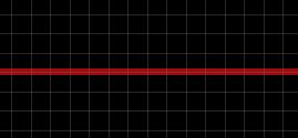
If the trace width is wider, it will result in a low impedance.
the trace width will be wider

If the trace width is narrow, it will result in a higher impedance.
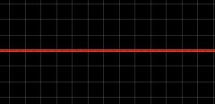
the trace width will be narrow
Visualization of Trace Spacing and Impedance:
Trace spacing and impedance in PCB design are closely related. For single-ended traces, the spacing affects crosstalk and overall signal integrity but doesn’t directly change the impedance. However, for differential pairs, the spacing directly influences the impedance. Closer spacing increases coupling and lowers impedance.
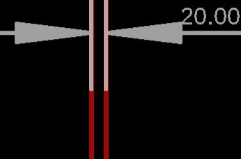
Closer spacing increases coupling and lowers impedance.

Closer spacing

Wider spacing decreases coupling and raises impedance.
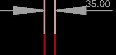
Wider spacing 1

Layer Stack up Techniques

The layer stack-up relates to the disposition of individual layers of a multi-layer PCB. To achieve the desired impedance control, it is possible to arrange the layers that carry signals in conjunction with the needed ground layers. For instance, the signal layers should be positioned near the ground planes so that there can be some stabilizing of the impedance as well as some sizable reduction in the signal noise.

Incorporation of Ground Planes

The addition of ground planes in the component design of the PCB also ensures the signals get a proper reference point and at the same time facilitates impedance control. It is an area of low impedance, signifying that ground planes lessen EMI and contribute to signal integrity by providing the signals with a low-impedance return path. The high-speed and high-frequency circuits benefit from this method due to the speed of convergence.

Impedance Matching Example: Controlling Impedance of 50 Ohm Transmission Line PCB

In high-frequency PCB design, achieving precise impedance control is crucial for signal integrity. Here, we present a practical example of controlling the impedance of a 50 ohm transmission line using specific parameters and calculations. This example focuses on design values, material properties, and the resultant calculations required to meet the impedance specification.

Design Parameters and Material Properties

Trace Geometry:
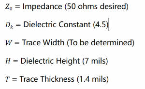
Initial Trace Width (W): Estimated at 10 mils
Material Properties:
  • Dielectric Constant (Dk): 4.5 (FR4)
  • Trace Thickness (T): 1.4 mils (1 oz. copper)
  • Dielectric Height (H): 7 mils (distance from the trace to the ground plane)
  • Target Impedance: 50 ohms
Calculation of Trace Width:
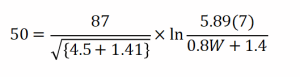
To achieve the desired impedance of 50 ohms, we use the following formula for a microstrip line:

Where:

notation

Now, Find the value of trace width by inserting the known values:
values
By solving the equation, the term W is found to be approximately 11.2 mils. To have an impedance of 50 ohms for a microstrip transmission line using PCB having FR4 material, the width of the trace should be approximately 11.
A trace thickness of 1 mil is needed to suit the dielectric height of 7 mils, and knowing that 2 mils is necessary. 4 mils. This calculation enables the check to be made to ensure that the impedance of the transmission line specified is achieved to provide signal integrity in high-frequency designs. 
But as all the theoretical calculations are made for a perfect world, in this case, the real manufacturing tolerances and environmental issues. It is suggested to perform the validation through the simulation and testing to ensure that the impedance of really existing structure corresponds to the calculated one concerning manufacturing errors.

Conclusion

Control of Impedance on the printed circuit boards or PCB is critical in high-frequency and high-speed electronics designs. The proper control of impedance guarantees that signals move along the PCB traces properly without being distorted, attenuated, or reflected; hence, signal integrity is achieved. There can be multiple ways of implementing the impedance control, few of them are listed here: 

  • Change in the trace width and space
  • Implementation of controlled dielectric materials 
  • Layer stack-up
The above-mentioned factors are well elaborated in the following example, explaining how these factors guarantee dependable performance in real-world applications. But the real manufacturing tolerances and environmental issues have to be compensated with the help of simulations and tests.
Want to get more expert suggestions of impedance control? Contact ELE PCB for support!

FAQs

Some of the familiar dielectric materials are FR4, Roger’s RT/duroid and Isola. All the materials have the dielectric constant (Dk) for impedance, thus it is significant to choose the correct type of material for the design.
Different temperature can affect the dielectric constant of many materials and the resistance of the traces that can lead to a change in the impedance. It is, therefore, required to take into account the corresponding temperature coefficients in the design to achieve stability of the impedance over the range of the temperature.
HyperLynx, one of the simulation tools, can be able to model and analyze impedance in PCB designs while ANSYS HFSS and Keysight ADS are other simulation tools that can perform the same function. Verification techniques include, for instance, Time Domain Reflectometry (TDR) and Vector Network Analyzer (VNA), mainly for real life measurement.
The thickness of a trace influences the impedance present in a circuit because it determines the resistance and inductiveness of the trace. Higher trace thickness is usually better because it is easier to handle lower impedance by way of reduced electrical resistance and greater ability to carry current while exact calculations must be done to obtain the precise amount of impedance wanted.
If the impedance is not correct, signal reflections can occur plus crosstalk and effective signal loss; this results to data loss, low performance or even a complete system breakdown. That is why it is critical to ensure the correct impedance when working with high-speed and high-frequency signals to protect signal integrity and the reliability of the system.

CONTACT US


We provide technical expertise form prototype through production, increasing speed to market by 20%.

                   Contact us below to start discussing your project with our Technical Experts today.

                   Whether you already have Gerber Files, submit a Quick Quote for free estimate.

Leo
I aim to bridge the gap between technical expertise and practical application, offering practical advice, best practices, and innovative ideas that inspire readers to push the boundaries of PCB design and embrace new possibilities.
About Benjamin

Benjamin is the general manager of ELE PCB, a leading PCB design and manufacturing company based in China. He has over 10 years of experience in the PCB industry, and has been involved in various projects.

Get a Quote
Recent Posts