Why Heavy Copper PCB Is Crucial for Efficient Power Management?
Table of Contents
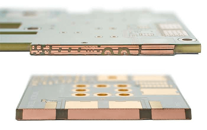
Heavy copper PCBs have a much thicker layer of copper foil than standard PCB board, and their characteristics of being able to bear heavier currents in the present and to better manage heat make them an inevitable option in such high-power application zones. These specialized PCBs are utilized particularly in power electronics, automotive, military, and renewable energy systems since these applications require significantly high dependability and high performance under intense conditions.
This article will introduce the definition, advantages, applications and design considerations of heavy copper PCB. Follow ELE now!
What is Heavy Copper PCB?
Heavy copper PCBs (printed circuit boards) have a copper foil thickness of more than 3 oz. In general, the thickness of the copper in traditional PCBs is between 1 oz to 3 oz per square foot. Yet, within heavy copper PCBs, the copper layer is about 4 oz/ft² and goes up to 20 oz/ft² or more based on the actual specifications of the given application.
Advantages of Heavy Copper PCB
Higher Currents Handling
The heavy copper PCB is in a position to support and handle far much higher electrical currents without the occurrence of a number of problems such as overheating and or high-performance compromise. It also improves the mechanical properties of the PCB, thus increases its capacity to endure a physically rigorous environment. Because of this, heavy copper PCBs are more applicable in circuits that implement large throughput of power, for example; industrial machines, car power supplies and high-power switching transducers.
Better Heat Dissipation
Moreover, if applied to current designs with heavier copper PCBs, heavy copper PCBs provide better heat dissipation. This is of special significance in power electronics, especially with heat, which poses a major challenge to the durability of the products. With thicker copper layers, these PCBs are capable of providing adequate heat-sinking and heat dispersion designed to keep the system cool as it occurs under conditions of higher loads.
Extended lifespan
Due to its thicker copper layer, heavy copper PCBs are more resistant to corrosion, heat and cold than general PCBs, and are often used in extreme environments. Due to these characteristics, thick copper PCBs also have a longer service life than other PCBs.
Design Considerations of Heavy Copper PCB
Although the manufacturing process of heavy copper PCBs is almostly the same as common PCBs, the deign process is different. You’d better take the following aspects into consideration to get a reliable copper PCB.
Copper Thickness
One of the most critical design factors for a heavy copper PCB is its copper thickness. Additional thicker copper helps the PCB provide much higher currents than its base materials would otherwise allow, but it also affects other design features such as the width of the traces or the space between them. When using thicker copper, the traces that connect different parts of the PCB should be made wider to accommodate it.
Wider traces are preferred because they reduce the resistance and stop the board from heat when it’s flowing large currents. On the other hand, if the traces are too narrow the resistance will be high can lead to heat generation which is not good for the board or may hamper the performance. Furthermore, as copper thickness gets bigger, you have to provide more space between the lines in order not to have shorting or even some electrical coupling that is undesired.
As a clearer picture of how copper thickness plays out to the design below is the following table that illustrates the copper thickness to minimum trace width and maximum current capacity. The figures in this table are general guidelines that engineers use to determine how wide the traces should be for a given copper thickness to safely carry a specific amount of current:
Copper Thickness (oz/ft²)
Minimum Trace Width (mm)
Maximum Current Capacity (Amps)
4 oz
1.5
10
6 oz
2.0
15
10 oz
3.0
25
20 oz
5.0
50
As shown in the table, a 4 oz copper layer requires a minimum trace width of 1.5 mm to handle 10 amps, while a much thicker 20 oz layer needs a 5.0 mm wide trace to safely carry 50 amps. This example highlights how critical it is to adjust trace widths based on the copper thickness to ensure the board operates efficiently and safely under high-power conditions.
Thermal Management
In high power electronic applications, thick copper pcbs experience high operational temperatures because of the large currents they conduct. Of particular note, these boards have multiple copper layers which can inherently help to dissipate heat but it is not enough to prevent high temperatures from arising. Other measures are required to help the PCB run optimally and safely and without getting too hot, or otherwise getting damaged.
Thermal Vias
Heat flow can be well controlled in a heavy copper PCB, one of the best ways being through the use of thermal vias. These are small Through Holes that are made from copper in the PCB; they function to transfer heat from high power density areas such as power components to other dissimilar planes or layers or even to a heat sink. Defining heat away from delicate items, the thermal vias do not allow the single points to become too hot and, instead, dissipate the heat far better around the copper.
Heat Sinks and Pads
The insertion of heat sinks or thermal pads is another vital part of agendas when it comes to thermal issues. Heat sinks are metallic pieces which mechanically mounted to the outer layer of the PCB to transfer heat away from devices such as power transistors or voltage regulators. Heating films, however, are typically located under such parts for better heat dissipation to the PCB or an external cooler. Altogether they will guarantee that the important components are at their permissible operational temperature even at increased electrical load.
Plating and Etching
The process or fabrication of heavy copper PCBs is slightly different from those of ordinary PCBs with simple copper shapes. Thick copper foils demand aggressive approaches to etching to create small features without under-etching the traces. In most cases, several cycles of plating are required to provide the needed thickness of copper on the component.
Plating: Dense copper layouts can call for several etching cycles to deposit the appropriate thickness of copper.
Etching: Vintage techniques in etching are required to make clean traces, mainly because copper thickness makes etching harder.
Via Design
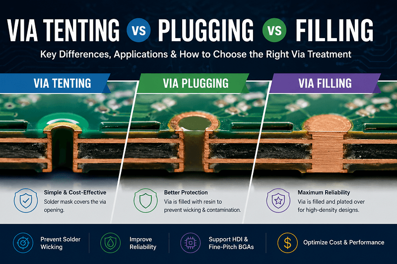
Vias are essential in any PCB, but in heavy copper designs, their ability to carry current and dissipate heat becomes even more critical. Larger or multiple vias are often necessary to handle the increased electrical and thermal loads.
Mechanical Strength
Heavily copper PCBs are manufactured to take demanding situations including mechanical shock, vibrations as well as fluctuations in temperatures. The thickness of copper layers in a layered board will always make the board strong, but one should still pay a lot of attention while designing the board so that the components do not move or get damaged while in use.
However, in regions of the PCB, where the circuit might be subjected to physical stressing such as bending or vibration, then the conductor traces should be wider and thicker. This helps guard against the vias and traces from cracking or getting damaged in the future, thus making sure the board is still dependable even where the environment is quite destructive.
Housings that can be physically stressed during operation, for example, power components or connectors, require solder joints with larger cross-sections. This makes certain that the component interconnections stay correctly soldered on the PCB, especially in times when there are rigorous and obtained conditions such as vibrations or mechanical shocks. Subsequently, it should be noted to properly pitch and reinforce key regions of the board, heavy copper PCB can be reliable mechanically as well as would endure dynamic campaigns.
Application of Heavy Copper PCB
Heavy copper-based PCBs are used in applications that call for increased power carrying capacity and ability to withstand harsh conditions of high temperatures, vibrations, amongst others. Here are some of the common industries where they are used:
Power Electronics
High copper PCBs are used in power supplies, inverters, and converters because control of large currents and the ability to efficiently shed heat are significant factors necessary for the functionality and reliability of PCBs.
Automotive Industry
In the areas of EVs, battery management systems, and charging stations, advanced and robust heavy copper PCBs are used to manage the high-power requirements and withstand automotive environments.
Solar Power and Renewable Energy
Such PCBs are employed in solar power systems as well as in the controllers and inverters in solar panels where the capacity to manage current and dissipate heat in a proficient and effective manner.
Industrial Control Systems
These PCBs are widely used in industries and motor controllers, power distribution systems, and many heavy devices for their endurance and efficiency of handling power on critical operations. Heavy copper printed circuit boards are used in shapes of high-power systems in many industries and therefore are a critical feature in achieving system reliability and robustness under conditions of high usage.
Military and Aerospace
It remains ideal for defence and aerospace industries because they offer excellent performance under varying harsh environmental conditions and currents required in the sector coupled with mechanical stresses ripped out from the two industries.
Conclusion
High copper PCBs are crucial in the PCB industry, which requires high power, thermal conductivity, and mechanical strength. Due to good design and fabrication, these products facilitate the safe passage of a large electrical current with excellent thermal characteristics, thus making essential power-oriented systems more reliable.
While selecting appropriate heavy copper thickness and focusing on thermal package challenges and mechanical structure, heavy copper PCBs contribute to improving product reliability, durability, and safety. If you want to find a reliable heavy copper PCB manufacturer, ELE PCB can provide heavy copper PCBs of different thickness and various layers. Every product of ELE will be under qualification tests to keep high-quality. Contact us to get further advice and a quick quote!
I aim to bridge the gap between technical expertise and practical application, offering practical advice, best practices, and innovative ideas that inspire readers to push the boundaries of PCB design and embrace new possibilities.
Benjamin is the general manager of ELE PCB, a leading PCB design and manufacturing company based in China. He has over 10 years of experience in the PCB industry, and has been involved in various projects.









 English
  Italian
  Hungarian