

Table of Contents
With the rapid increase in signaling speeds, the PCB also puts forward higher requirements. Printed circuit boards provide circuit performance that must be able to make the signal in the transmission process not occur reflection phenomenon, the signal remains intact, reduces transmission loss, and plays the role of matching impedance so that we can get a complete, reliable, accurate, non-interference, noise transmission signal.
Impedance control affects the proper operation of electronics in the context of printed circuit boards or PCBs. Let’s now examine what PCB impedance control entails and the reasons behind its importance.
Understanding PCB Impedance Control

Why PCB Impedance Control is Important in PCB Design?

- Signal Integrity (SI): Impedance control is critical to maintaining signal integrity. In high-speed circuits, the rise time of the signal is very short, and the signal has a high-frequency component. If the impedance is not properly controlled, the signal will reflect and distort the transmission line, resulting in signal integrity problems.
- Reducing Signal Reflections: Reflections occur when a signal encounters an abrupt change in impedance. Proper impedance control reduces such reflections and ensures smoother transmission of signals through the circuit, reducing false signals caused by reflections.
- Reduce Electromagnetic Interference (EMI): Impedance mismatch will increase electromagnetic radiation, thus increasing EMI. Controlling impedance helps to reduce EMI, which is important for meeting Electromagnetic Compatibility (EMC) standards.
- Improving System Performance: In high-speed data transmission and high-frequency signal processing, impedance control can improve the bandwidth and performance of the system, reduce signal attenuation, and ensure the accuracy and reliability of data transmission.
- Impedance Matching: Impedance matching is the key to ensuring the smooth transmission of signals between different circuit elements. If the impedance of the transmitter and receiver are not matched, energy loss and signal distortion will result.
- Design and Manufacturing Complexity: Impedance control requires designers to take into account a variety of factors at the design stage, such as alignment width, dielectric thickness, dielectric constant, and so on. At the same time, the manufacturing process also needs to be strictly controlled to ensure the consistency of impedance.
- Special Requirements for High-Frequency Applications: Impedance control is especially critical in high-frequency applications. For example, in radio frequency (RF) and microwave circuit design, impedance control is directly related to the resonant frequency and bandwidth of the circuit.
- Testing and Verification: Impedance control also needs to be verified by specialized test equipment, such as network analyzers, to ensure that the PCB’s impedance characteristics meet design requirements.
- Cost and Reliability: Although precise impedance control may increase the cost of design and manufacturing, it can significantly improve product reliability and performance, reducing rework and failure rates.
- Technical Challenges: Impedance control involves technical challenges in several areas, including materials science, electromagnetic, and manufacturing processes. As electronic devices evolve to higher speeds and smaller sizes, the difficulty of impedance control increases.
Factors Affecting Impedance in PCB Manufacturing

Controlled Dielectric Constant
Line width
Line thickness (line copper thickness)
Dielectric Constant
Solder mask Thickness
Explore the Methods of Impedance Control
Based on the literature review, the following methods have been identified to control impedance.
Controlled Dielectric Constant
Trace Width and Spacing Adjustments
How Trace Width Affects the Impedance?
How Trace Spacing Affects the Impedance?
Balancing Trace Width and Spacing
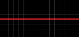
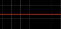
If the trace width is narrow, it will result in a higher impedance.
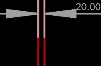
Closer spacing increases coupling and lowers impedance.
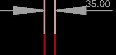
Wider spacing decreases coupling and raises impedance.
Layer Stack up Techniques
Incorporation of Ground Planes
Impedance Matching Example: Controlling Impedance of 50 Ohm Transmission Line PCB
Design Parameters and Material Properties
- Dielectric Constant (Dk): 4.5 (FR4)
- Trace Thickness (T): 1.4 mils (1 oz. copper)
- Dielectric Height (H): 7 mils (distance from the trace to the ground plane)
- Target Impedance: 50 ohms
Where:
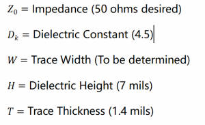
Now, Find the value of trace width by inserting the known values:
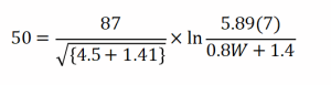
A trace thickness of 1 mil is needed to suit the dielectric height of 7 mils, and knowing that 2 mils is necessary. 4 mils. This calculation enables the check to be made to ensure that the impedance of the transmission line specified is achieved to provide signal integrity in high-frequency designs.
Conclusion
Control of Impedance on the printed circuit boards or PCB is critical in high-frequency and high-speed electronics designs. The proper control of impedance guarantees that signals move along the PCB traces properly without being distorted, attenuated, or reflected; hence, signal integrity is achieved. There can be multiple ways of implementing the impedance control, few of them are listed here:
- Change in the trace width and space
- Implementation of controlled dielectric materials
- Layer stack-up
FAQs


CONTACT US





 English
  Italian
  Hungarian