

Table of Contents
Why Do We Need PCB Inspection?
PCB Inspection is one of the most essential parts of the PCB manufacturing process.
It involves checking printed circuit boards for defects and errors, and ensuring they comply with design specifications.
PCB Inspections are important for reasons below:
- Aviod PCB defects or failures
- Check PCB for acceptable standards
- Keep stable high-quality
- Save repairing costs afterwards
- Increase product quanity
- Improve clients’ satisfication
Types of PCB Defects
In PCB manufacturing, various PCB defects could arise. This could affect the performance and reliability of electronic devices. Some of such PCB defects include:
- Soldering Defects
- Component placement errors
- Missing components
- Insufficient solder or solder bridges
- Open circuits
- Short circuits
- Solder mask issues
- Copper trace discontinuity
- Incorrect component values or orientations
PCB Inspection Methods
During the production and assembly of printed circuit boards (PCBs), there are various inspection methods to ensure their quality and reliability. Here are some common PCB inspection methods:
Manual Visual Inspection
Manual Visual inspection is a fundamental method for examining Printed Circuit Boards (PCBs) in the electronics manufacturing process. This method involves carefully inspecting the PCB for any visible defects. The defects include soldering irregularities, component misalignment, missing components, or physical damage. Skilled technicians use circuit board inspection camera and microscopes to ensure a detailed examination.

The advantages of AOI are that it requires less equipment, low cost and can detect some significant defects. However, manual inspection is more time-consuming and prone to error than machine inspection, and it is difficult to detect internal or tiny defects.
Automated Optical Inspection (AOI)
It is a modern method that uses AOI machines with cameras and smart image analysis to check PCBs. AOI systems quickly review the entire board to find problems like bad soldering, missing parts, or things in the wrong place. These machines can notice tiny issues that humans might miss. This makes the evaluation more detailed and reliable.

AOI works well for inspecting a lot of PCBs quickly and accurately, especially in big productions. AOI systems also use AI and machine learning. This means they get better at finding problems over time.
Manual Visual Inspection vs Automated Optical Inspection
| Manual Visual Inspection | Automated Optical Inspection (AOI) |
| Inspected by human eyes | Uses specialized machines with cameras |
| Relies on visual scrutiny | Utilizes image processing algorithms |
| Prone to human error | Provides rapid and consistent scanning |
| Limited to human speed | Detects minute discrepancies |
| Subjective interpretation | Enhances efficiency and accuracy |
| Suitable for small batches | Particularly effective in high-volume production |
| Time-consuming | Integrates AI and machine learning for improved accuracy |
Automated X-ray Inspection (AXI)
Automated X-ray inspection is a non-destructive approach for inspecting PCB interior structures. This approach is useful for detecting hidden problems beneath the surface. It can uncover issues like soldering voids, component connections, and probable manufacturing difficulties. X-ray machine for PCB produces images that allow inspectors to see the PCB’s internal layers. This is accomplished without physically disassembling the device.

This strategy is beneficial for complex multilayer PCBs with limited visibility and inspecting solder bridges under BGA components.
X-ray inspection for electronic components can ensure the integrity of components, so X-ray examinations are critical in areas where precision and dependability are critical, such as aerospace or medical devices.
Functional Testing
Functional testing is a flexible method for PCB examination. Its primary goal is to ensure that the built board executes its intended tasks correctly. This procedure applies electrical signals to the PCB, and the output is monitored to ensure it meets design standards. Functional testing can detect flaws such as broken components, circuitry defects, or connectivity issues by imitating real-world working situations.

Functional testing gives a thorough evaluation of the PCB’s functioning. However, it may not identify individual component-level flaws. This procedure is frequently used as the last stage in the inspection process. It confirms the general operation of the PCB before it integrates into the final product.
In-Circuit Testing (ICT)
This method inspects individual components and their connections on a PCB, while the board is powered. Specialized test probes are used to get access to specific spots on the circuit and assess electrical parameters. ICT is effective at detecting problems such as open circuits, short circuits, and component value variations.

While it provides comprehensive coverage, ICT may not be effective for discovering faults in places with limited access. ICT is often used for medium to high-volume production runs, and it assists in ensuring the electrical integrity of the PCB before it moves on to the next manufacturing stage.
Thermal Imaging
Thermal imaging is a non-contact PCB inspection technique that uses infrared cameras to find temperature differences on a PCB’s surface. This technique is useful for detecting problems such as overheating components, improper connections, or insufficient heat dissipation.

Thermal imaging can detect abnormalities that could suggest future failures or areas of concern. It is especially beneficial in applications requiring temperature stability, such as power electronics or high-performance computers. Thermal imaging enhances the overall PCB dependability in a variety of electronic systems by enabling the early detection and resolution of possible thermal problems by giving a visual depiction of the temperature distribution.
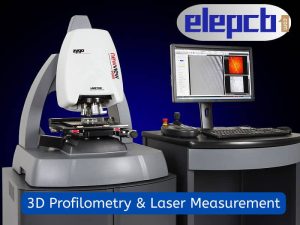
3D Profilometry and Laser Measurement
Methods of 3D profiling and laser measurement of PCBs include light projection to create 3D models, and laser projection combined with camera imaging to take accurate measurements. These advanced 3D inspection and analysis techniques are ideal for examining PCBs with intricate and dense structures, enhancing PCB quality, and aligning with the AI and robotics industries.
PCB Inspection Standards
Several widely recognized standards guide PCB inspection practices in the electronics industry. Some of them include:
IPC-A-600:
- Acceptability of Printed Boards Standard
- Defines the acceptance criteria for bare printed boards.
- Specifies requirements for base materials, conductor patterns, holes, and other features.
IPC-A-610:
- Acceptability of Electronic Assemblies Standard
- Outlines acceptability criteria for assembled PCBs.
- Categorizes defects into different classes based on their impact on performance and reliability.
IPC-6012:
- Focuses on qualification and performance specifications for rigid PCBs.
- Provides requirements for base materials, design, construction, and final finish.
J-STD-001:
- Establishes requirements for the soldering process in electronic assemblies.
- Details criteria for various soldering classes based on the application and end-user requirements.
ISO 9001:
- A broader standard covering quality management systems applicable to various industries, including electronics manufacturing.
- Emphasizes continuous improvement, customer satisfaction, and adherence to processes and standards.
UL 796:
- Addresses the safety aspects of printed wiring boards.
- Provides requirements for flammability, electrical tracking, and resistance to solvents.
Future Trends in PCB Inspection
In the near future, a spike in sophisticated automation in the future of PCB inspection could be observed. This automation will use artificial intelligence and robotics to conduct faster, more exact exams. Machine learning will make inspection systems more intelligent. They will be capable of identifying and responding to changing flaws. This would allow for real-time monitoring and analysis of production processes.
Intelligent data analytics will extract important insights from inspection data, allowing for predictive maintenance and continual process improvement.
As electronic components continue to shrink, PCB inspection technology will evolve to become more sophisticated, capable of detecting more subtle defects. Additionally, inspection systems and other stages of the manufacturing process will be integrated to create a more efficient production system.
Furthermore, a future emphasis on sustainability may lead to using environmentally friendly materials and techniques in PCB inspection, which would coincide with broader environmental aims.
Conclusion
PCB inspection serves as a gateway to quality assurance in the electronic industry. By implementing advanced PCB inspection techniques like AOI and X-ray PCB inspection, manufacturers can enhance the accuracy of PCB. The electronic manufacturing industry may continue to push the frontiers of innovation. It may also maintain the highest quality and reliability. This requires a thorough understanding of PCB inspection methods and defect kinds.
Thus, ELEPCB will elevate your electronic manufacturing with advanced PCB inspection techniques. Explore the power of AOI, X-ray PCB inspection and more for your accuracy and reliable PCB product with ELEPCB. Contact us today for expert guidance and advanced solutions in PCB inspection.


CONTACT US



 English
  Italian
  Hungarian